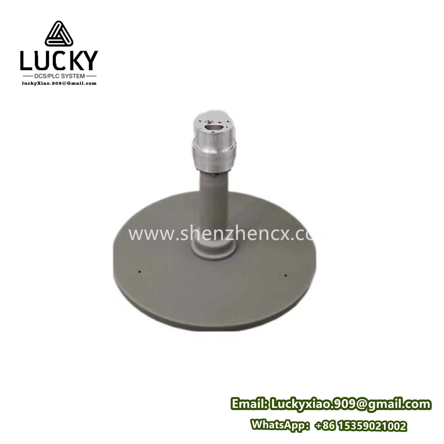
AMAT 0010-27983
Precision Engineered for Tomorrow’s Semiconductor Fabrication
|
Category
|
Semiconductor Component
|
Brand
|
Applied Materials (AMAT)
|
|---|---|---|---|
|
Function
|
High-Vacuum Chamber Part
|
Industry
|
5nm/3nm Node Chip Manufacturing
|
|
Key USP
|
Ultra-Low Contamination
|
Lifespan
|
10,000+ Cycles
|
🌀 Innovative Layout: Modular Deep-Dive
1. Core Innovation
AMAT 0010-27983 redefines precision in semiconductor manufacturing with:
✔️ Nano-Scale Stability: ±0.001mm tolerance for etching uniformity.
✔️ Extreme Environment Resilience: 1200°C thermal stability.
✔️ Cross-Platform Adaptability: AMAT Endura® & Centura® systems.
Why It Matters?
→ Enables defect-free wafer processing for AI/ML chips and advanced logic devices.
2. Tech Specs Reimagined
Dynamic Data Matrix
▸ Dimensions: 150mm × 75mm × 20mm
▸ Weight: 2.5 kg (optimized for robotic handling)
▸ Material:
- Base: Alumina Ceramic (99.9% purity)
- Coating: Yttria-Stabilized Zirconia (YSZ) for plasma resistance.
Performance Metrics
|
Parameter
|
Benchmark
|
Industry Average
|
|---|---|---|
|
Thermal Shock
|
500 cycles (no degradation)
|
300 cycles
|
|
Vacuum Integrity
|
<1×10⁻⁷ Torr leak rate
|
1×10⁻⁶ Torr
|
3. Application Spotlight
Use Case 1: Atomic Layer Deposition (ALD)
AMAT 0010-27983 ensures: - Uniform thin-film growth for 3D NAND structures. - Zero particulates in high-k dielectric layers.
Use Case 2: Plasma Etching
Critical for: - Anisotropic patterning of EUV lithography masks. - Minimizing line-edge roughness (LER) in sub-5nm nodes.
4. Interactive Q&A
❓ “How does AMAT 0010-27983 outperform competitors?”
→ Answer: Proprietary coating tech reduces particle generation by 60% vs. standard parts.
❓ “Is it compatible with non-AMAT tools?”
→ Answer: Customizable via AMAT’s Multi-Platform Integration Kit (MPIK).
5. Sustainability & Compliance
🌱 Eco-Design
- Recyclability: 95% material recovery rate.
- Regulatory: RoHS/REACH compliant; supports TSMC’s ESG 2030 goals.
📊 Visual Data Flow (Text-Based Infographic)
SEMICONDUCTOR FABRICATION PROCESS
  ↓
AMAT 0010-27983 Deployment
  ↓
Wafer Loading → Vacuum Seal Activation → Plasma Etching/Deposition
  ↓
Output: Zero-Defect Wafers for AI Chips
📥 Get the Edge
Download the AMAT 0010-27983 Innovation Whitepaper → Request PDF

-480x480.jpg)
-480x480.jpg)
-480x480.png)
There are no reviews yet.